10+ Adder Circuit Diagram. The main disadvantage of this circuit is that it can only add two inputs and if there is any carry, it is neglected. Adders, subtractors, ripple adders carry look ahead adders.
Full Adder Conbinational Circuit ~ All Computer Topics from 1.bp.blogspot.com
Bcd adder truth table and bcd adder block diagram which gives you detail. Full adder from 2 half adder. An electronic or digital circuit that performs addition of two binary numbers and is a type of adder is known as a half adder.
In the half adder circuit the sum and carry bits are defined as.
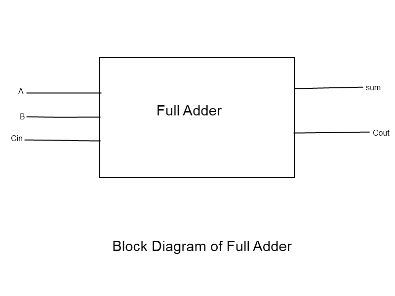
10+ Adder Circuit Diagram. The full adder circuit diagram add three binary bits and gives result as sum, carry out. Let's see the block diagram, full adder circuit construction is shown in the above block diagram, where two half adder circuits added together with a or gate. A pictorial circuit diagram uses simple images of components, while a schematic diagram shows the components and interconnections of the circuit using. It has xample full adder logic diagram;