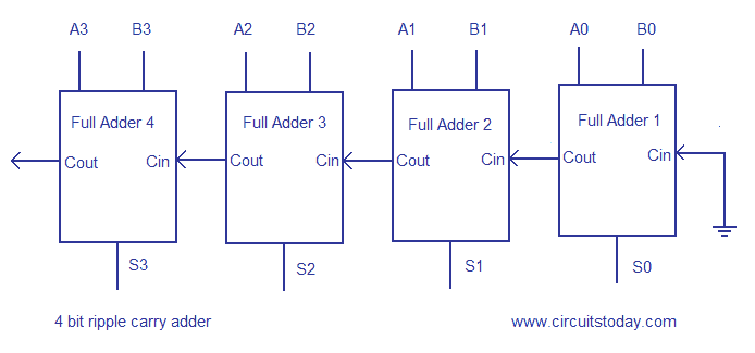
10+ Circuit Diagram Of Full Adder. Full adder is developed to overcome the drawback of half adder circuit. You can easily design the full adder circuit by practicing the exercises given below.
Stuck at Testing of Digital Combinational Logic Part 2 from accendoreliability.com
Circuit diagram of a full adder. We can verify it easily from the above circuit diagram or from the boolean functions of outputs of full adder. There is a control line k that holds a binary value of either 0 or 1 which determines that the operation being carried out is addition or subtraction.
From the function palette on the block diagram window select boolean and then select exclusive or as the complete block diagram of a full adder is shown in the figure below
10+ Circuit Diagram Of Full Adder. We can verify it easily from the above circuit diagram or from the boolean functions of outputs of full adder. Full adder definition, block diagram, truth table, circuit diagram, logic diagram, boolean expression and equation are discussed. Consider adding two binary numbers together: As shown in the figure, the first full adder has control line directly as its.