11+ Mux Logic Diagram. 2:1 mux verilog in data flow model is given below. We can easily understand the operation of the above circuit.
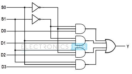
A logic block is diagrammed as a box. Block diagram, truth table, working and logic diagram of 1 to 4 demultiplexer. The circuit diagram of 4×1 multiplexer is shown in the following figure.
Simplifying design with 1.8 v logic muxes and switches.
11+ Mux Logic Diagram. Use creately's easy online diagram editor to edit this diagram, collaborate with others and export results to multiple image formats. You need a combinational logic with 16 input pins, 4 select lines but you'd then have a logic with 4 output pins. A logic block has inputs & outputs, which are done with wires. Use creately's easy online diagram editor to edit this diagram, collaborate with others and export results to multiple image formats.