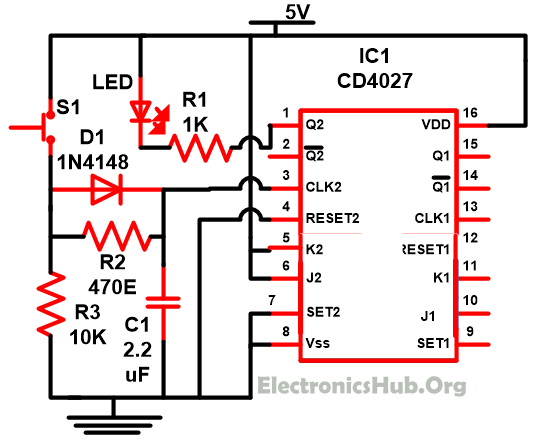
12+ Jk Flip Flop Diagram. As told earlier, j and k will be given as external inputs to s and r. It operates with only positive clock transitions or negative clock transitions.
It has two stable states high and low i.e. When the clock pulse is high the output of. Jk flip flop timing diagram.
You can show on the right the timing diagram of the.
12+ Jk Flip Flop Diagram. When the clock pulse is high the output of. Now, we shall verify our system so as to ensure that it behaves like we expect it to. A flip flop is a binary storage device. The first task is relativly straight forward.