13+ 3 Bit Odd Parity Generator Circuit Diagram. Of proposed parity bit generator circuit, design based on ptl. (iii) apply the inputs and verify the truth table for the parity generator.
(ii) for all the ics 7 th pin is connected to ground and 14 th pin is given +5v supply. • verbal description of the function of the final circuit. (iii) apply the inputs and verify the truth table for the parity generator.
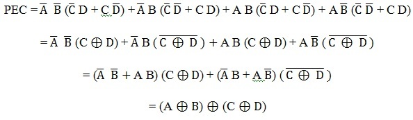
A parity bit, or check bit, is a bit added to a string of binary code.
13+ 3 Bit Odd Parity Generator Circuit Diagram. • verbal description of the function of the final circuit. The parity generator circuit will take 3 input bits, x, y, and z, and produce 1 output bit,, p. Parity generator, parity checker also can be even or odd and this even or odd is depending on the kind of extra bit generated at the sender's end. The logic diagram is as shown.