13+ Pt2313 Circuit Diagram. Pt2313 application circuit are optimized for easy pcb layout and cost saving advantage for audio Shows how to brighten and dim and led using pulse width modulation.
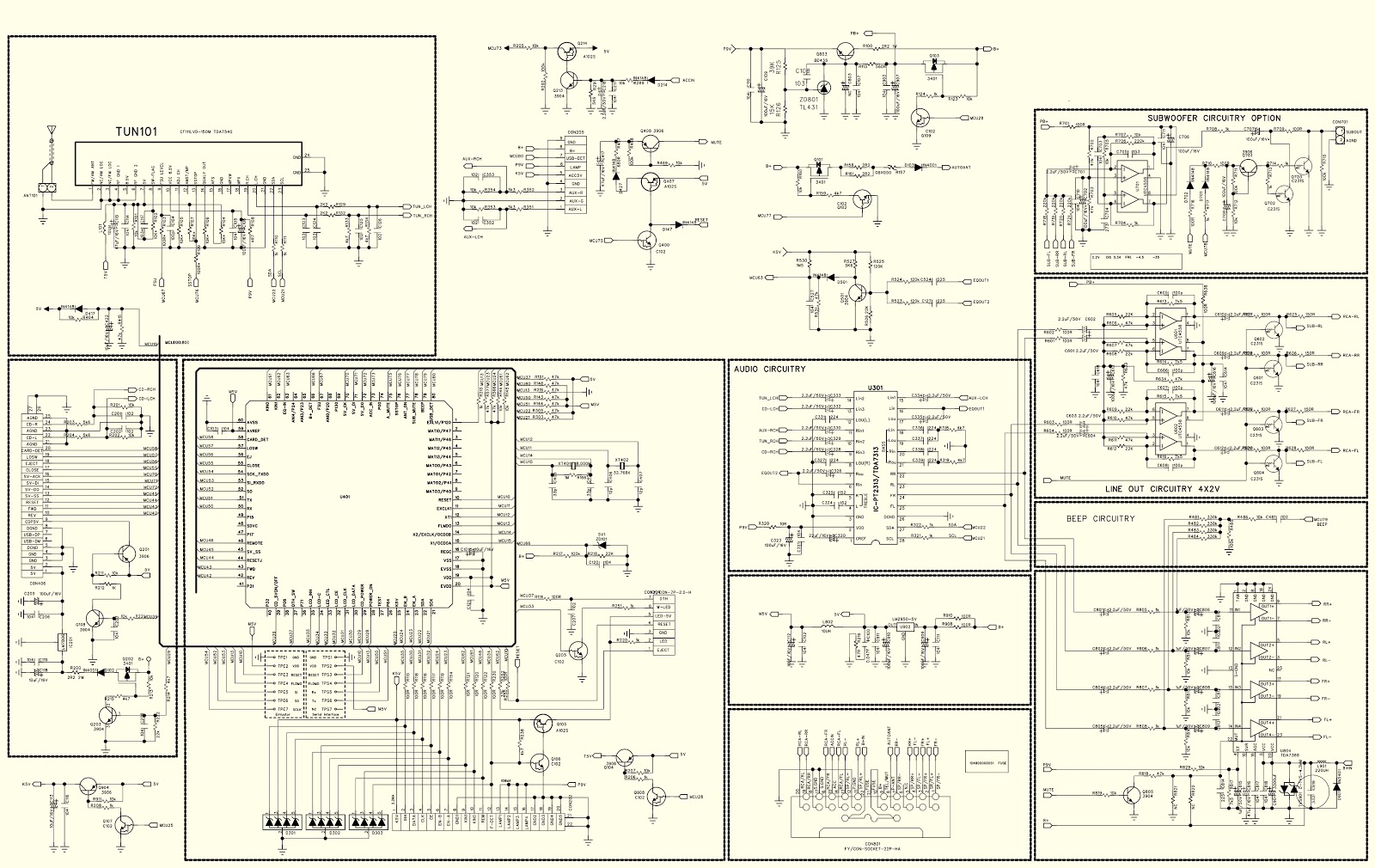
Volume, bass, balance, front/rear fader processor, selectable input gain are incorporated into a single chip having the highest performance and reliability with the least external components. So please wait i test it (and prolly fix) before use it with energia mcu's! Pt2313 application circuit are optimized for easy pcb layout and cost saving advantage for audio
Pt2313 application circuit are optimized for easy pcb layout and cost saving advantage for audio
13+ Pt2313 Circuit Diagram. The pwm output is obtained from the oc0a output of timer/counter0 which is on pb2, pin 14 of the attiny2313. The pwm output is obtained from the oc0a output of timer/counter0 which is on pb2, pin 14 of the attiny2313. Pt2313 application circuit are optimized for easy pcb layout and cost saving advantage for audio Soldering pt2313l using fingers 2019_news today infor.
Recent search terms:
- pt2313 arduino
- ta2926hq amplifier circuit
- tda7388 схема усилителя своими руками