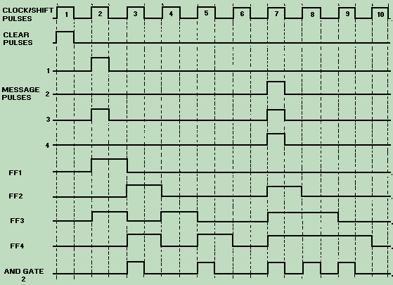
15 Parallel In Serial Out Shift Register Timing Diagram. Some of the features of 74hc165 to control the shift register, you would need three pins which are parallel load input (pl), clock input (cp) and clock enable input (ce). Shift/serial load— data present on the si pin shifts into the register on the falling edge of cp.
Shift registers from www.tpub.com
We enter a four bit binary. Shift registers can have both parallel and serial inputs and outputs. Browse shift register ic products from ti.com.
Some of the features of 74hc165 to control the shift register, you would need three pins which are parallel load input (pl), clock input (cp) and clock enable input (ce).
15 Parallel In Serial Out Shift Register Timing Diagram. Shifting out & the 595 chip. This block outputs a vector of last n samples of the input signal. 74hc165 parallel in, serial out shift register. Shifting out & the 595 chip.