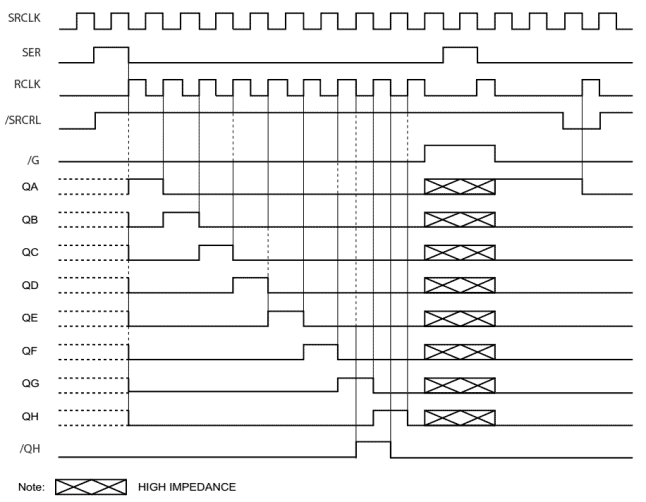
11+ Shift Register Timing Diagram. Regardless of if the data is loaded in all at once via parallel load or one bit at a time data is than shifted to the next flip flop with each clock pulse. The shift register is a sequential logic circuit which is used for the storage or the transfer of data in the form of binary numbers.
Daisy-chained 74HC595s controlled by SPI on STM32F4 – part … from elektronotes.files.wordpress.com
Each for loop is going to shift one bit of the value at a time into the register. Learn how shift registers are made of logic devices as she breaks down the logic diagrams and shows how to read the timing diagrams to. Today, i will explain how to figure out what a shift register needs and then show what that looks like in code and on the breadboard.
Question 1 complete the timing diagram for this circuit, assuming all q outputs begin in the low state
11+ Shift Register Timing Diagram. You will be presented with a diagram similar to the one shown below. We have not looked at asynchronous loading of data up to this point. This code is given to me for shift register entity shift4 is. Shift registers are devices that are quite popular when using micro controllers as they can be used to expand the number of inputs or outputs available.